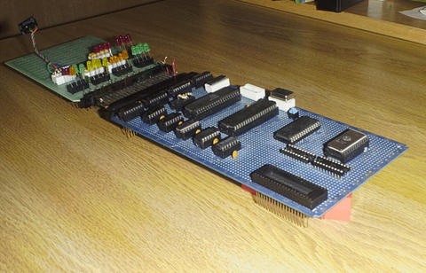
Apple I Processor Section
I have attempted a redesign of the Apple I processor section. It is available in PostScript:
Processor Section Redesign (PS)
The schematic was designed in XCircuit using Fink.
The design includes a 6502 processor, 6821 PIA, CY6264 8Kx8 Static RAM, and a 2716 EPROM. This is the first design I've worked on that uses a processor or memory, so it is quite likely I have made some glaring errors. I am very appreciatived of any feedback. Comments can be posted here.
The Design
EPROM
The ROM monitor is at addresses FF00.FFFF. In place of two PROMs, a 2716 EPROM is used. On the EPROM, address lines A0-A7 are connected to the processor's address lines. A8-A10 are tied to ground. /CE is low when A8-A15 are all high. /OE is connected directly to the processor's R/W. All data lines are directly connected to the processor.
RAM
The Apple I has 8k of RAM, provided by 8 8kx1 dynamic RAM package. These are replaced with one 8kx8 static RAM package, the CY6264. This eliminates the need for the RAM refresh circuitry. The RAM is at addresses 0000.0FFF (for sysem and user) and E000.EFFF (for BASIC). A0-A11 are connected to the processor address lines. A12RAM = (A12' • A13 • A14 • A15). CE2 = (A12' • A13' • A14' • A15' + A12' • A13 • A14 • A15). /CE1 is tied to ground (why are there two chip enables?). /WE is connected to the processor's R/W. /OERAM = R/Wproc and /WE = R/Wproc'. All data lines are connected directly to the processor.
Processor
Ø0 connects to the time base generation circuit provided in the Rockwell data sheet. /NMI, /IRQ, /ML, RDY, and /RES are all tied high. SYNC and Ø1 have no connection. Much thanks goes to Michael Rothe for help with the clock.
PIA
The 6820 is replaced with the externally identical 6821. /IRQA, /IRQB, and CA2 have no connection. CS1 is high. CS0 is connected to the processor's A4, RS1 to A1, and RS0 to A0. CS2 = (A15 • A14 • A13' • A12). All data lines are connected to the processor's. R/W is connected to R/Wproc. E is connected to Ø2. The keyboard connection (PA0-PA6) is wired for an Apple II+ keyboard. PA7 is wired high.
The terminal section is presently configured to use a printer for output, which will allow testing of the processor section independent of the terminal section. The printer wiring is based on this schematic. CB2 sends the "Data Ready" signal to the printer. CB1 and PB7 are low when "Data Accepted" is high.


Comments
Cool!
So, can you use this as a full Apple I, or do you have to add video board, etc?
Video
You'd have to add video circuitry if you wanted video output. Keyboard input works, but the only output is the LEDs you see, which are hooked up to the address and data lines.
Vince Briel has a video circuit on a microcontroller which he uses for his Replica I. That chip would work with this design as well.
schematics
when I try to view these files it looks like the drawing has been cut in half, only the section with the keyboard connector and (mostly) the PIA show up, what gives?
Re: schematics
When I downloaded the pdf, it was cut in half, but the postscript looked fine.